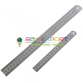
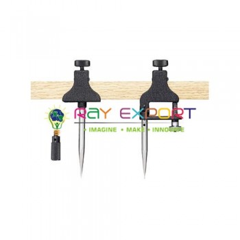
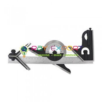
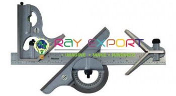
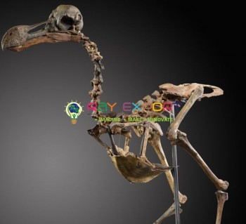
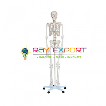
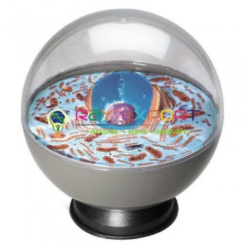
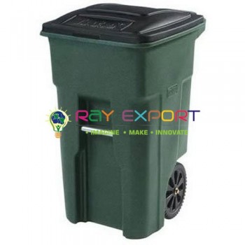
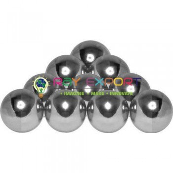
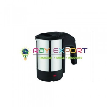
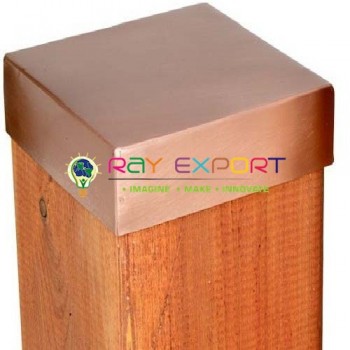
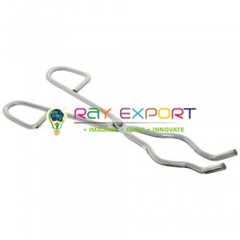
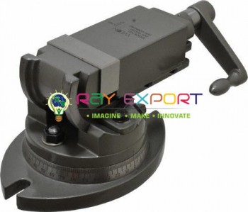
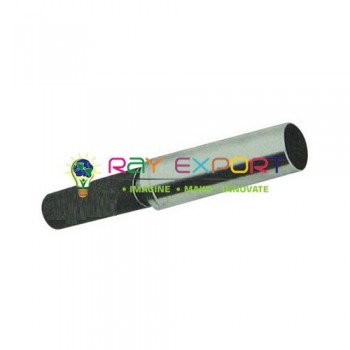
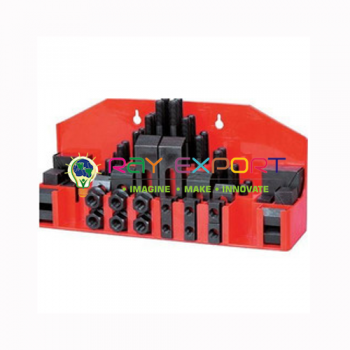
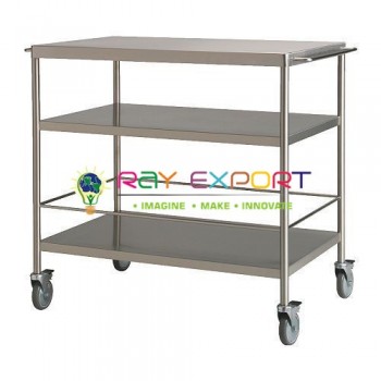
Ray Export is a leading manufacturer, supplier and exporter to following countries : India, Afghanistan, Albania, Algeria, Andorra, Angola, Antigua and Barbuda, Argentina, Armenia, Australia, Austria, Azerbaijan, Bahamas, Bahrain, Bangladesh, Barbados, Belarus, Belgium, Belize, Benin, Bhutan, Bolivia, Bosnia and Herzegovina, Botswana, Brazil, Brunei, Bulgaria, Burkina Faso, Burma/ Myanmar, Burundi, Cambodia, Cameroon, Canada, Cape Verde, Central African Republic, Chad, Chile, Colombia, Comoros, Congo, Congo, Costa Rica, Cote d'Ivoire/Ivory Coast, Croatia, Cuba, Cyprus, Czech Republic, Denmark, Djibouti, Dominica, Dominican Republic, East Timor, Ecuador, Egypt, El Salvador, Equatorial Guinea, Eritrea, Estonia, Ethiopia (Addis Ababa), Fiji, Finland, France, Gabon, Gambia, Georgia, Germany, Ghana, Greece, Grenada, Guatemala, Guinea, Guinea-Bissau, Guyana, Haiti, Honduras, Hungary, Iceland, Indonesia, Iran, Iraq, Ireland, Israel, Italy, Jamaica, Japan, Jordan, Kazakstan, Kenya (Nairobi), Kiribati, Korea, North, Korea, South, Kuwait, Kyrgyzstan, Laos, Latvia, Lebanon, Lesotho, Liberia, Liechtenstein, Lithuania, Luxembourg, Macedonia, Madagascar, Malawi (Lilongwe), Malaysia (Kuala Lumpur), Maldives, Mali, Malta, Marshall Islands, Mauritania, Mauritius, Mexico, Micronesia, Moldova, Monaco, Mongolia, Montenegro, Morocco, Mozambique, Namibia, Nauru, Nepal, Netherlands, New Zealand, Nicaragua, Niger, Nigeria (Abuja), Norway, Oman, Palau, Panama, Papua New Guinea, Paraguay, Peru, Philippines (Manila), Poland, Portugal, Qatar, Romania, Russia, Rwanda (Kigali), Saint Kitts and Nevis, Saint Lucia, Saint Vincent and the Grenadines, Samoa, San Marino, Sao Tome and Principe, Saudi Arabia, Senegal, Serbia, Seychelles, Sierra Leone, Singapore, Slovakia, Slovenia, Solomon Islands, Somalia, South Africa, South Sudan, Spain, Sri Lanka, Sudan, Suriname, Swaziland, Sweden, Switzerland, Syria, Tajikistan, Tanzania, Thailand, Togo, Tonga, Trinidad and Tobago, Tunisia, Turkey, Turkmenistan, Tuvalu, Uganda (Kampala), Ukraine, United Arab Emirates (Dubai), United Kingdom (London), United States, Uruguay, Uzbekistan, Vanuatu, Venezuela, Vietnam, Yemen , Zambia (Lusaka), Zimbabwe